Wafer fabrication
How a wafer fab gets from a defect map to the steps worth checking first
Talk to an engineer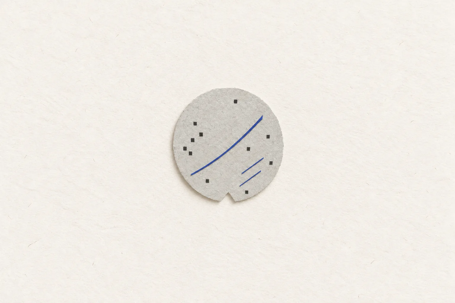
- Shape → mechanism
- reads the likely cause from how the tracks run, and rules out explanations that don’t fit
- Where to look first
- candidate process steps and parts, ranked, each with its reasoning and checks
- Engineers confirm
- every lead shows its reasoning; engineers settle which tool, and what fix, on the floor
At this wafer fab, inspection tools say whether a wafer has defects and, at best, what kind. Finding which step and which part caused them meant waiting for a senior expert or a process engineer to read the pattern and dig through the wafer’s history. In this collaboration, engineers can hand the map to Micius first. It infers the likely cause from the shape of the tracks and ranks what to check, for engineers to verify on the floor.
Challenge
From what the defect is to why it happened
An inspection tool scans a wafer, and the defect map shows a long, thin arc and straight lines with stray particles around them. Conventional inspection and classification tools stop about there: they flag the wafer and, at most, label the pattern a scratch. Engineers need the next answers. Which step, and which part, made the scratch, and how do they stop it happening again?
A senior defect expert or a process or integration engineer used to work these out. They read the pattern from experience, then went into YMS, the yield management system, and MES, the manufacturing execution system, for the wafer’s history: which parts it met, which steps and recipes it ran through. The hard part is the reasoning in between, from pattern to mechanism to a specific step and part. It comes from years of seeing similar cases, and only a handful of people have it, so the tools keep producing maps faster than anyone can explain them.
Solution
Reading the cause from the shape of the tracks
An engineer uploads the map and asks what the defect is and which step might have caused it. Micius, which has knowledge of semiconductor processes and defect mechanisms, reads the spatial pattern first: how many tracks, arcs or straight lines, continuous or broken, and whether the background particles matter. It marks the dies each track crosses and lists what it sees beside the map: one long arc centred off the wafer, two almost parallel straight lines, scattered particles elsewhere. Fine, continuous, long tracks are not what random scatter produces, so Micius calls it a scratch.
Illustrative flowIt reads the shape and spread of the tracks, then calls it a scratch.
Then it reasons about the mechanism. Long, continuous tracks point to something solid touching the wafer surface. Straight lines are typical of transfer, where the wafer slides against a fixed edge or obstacle. An arc suggests rotation about some axis: a swinging part, a particle caught during CMP, a turning robot. Because this arc is centred off the wafer, the wafer simply spinning on its chuck is unlikely. Micius also says what doesn’t fit. Airflow problems tend to leave wider marks with a clear direction, and chemical problems tend to form concentric rings; neither pattern appears on this map, so Micius sets both aside and leaves transfer steps and rotating ones to check.
Illustrative flowLines and an arc each point to a kind of step; airflow and chemistry are ruled out.
Leads
A ranked list of what to check first
Micius ranks the process steps and parts most likely to be involved, each with its reasoning, an alternative and a first check. Here that meant starting with the height and swing path of a nozzle arm in the clean module, then the robot’s pick-and-place height. The checks are specific enough to act on: particles on the robot blade, recent handling alarms, burrs or debris in a cassette slot.
It is also clear about what the ranking rests on. It had the map and its process knowledge, nothing else: it didn’t know which inspection step produced the map, hadn’t seen the wafer’s process history, queried no system and changed no tool or parameter. It suggested pulling the maps for the other wafers in the lot, since several scratches in about the same place would point to a tool rather than a one-off, and left that comparison to the engineers. The reply ends with a note that the list is to be checked on the floor.
Results
Engineers start from a reasoned list
From one map, Micius can point only to a kind of step and a kind of part. Which tool it actually was, what to check first and what to do about it are settled by engineers on the floor. In the collaboration with this fab, Micius gives the first read. Senior experts and process and integration engineers check its reasoning, then decide which tool and part to look at, so their experience goes into confirming and deciding instead of working out every map from scratch.
What’s next
Narrowing a lead to one tool
Pinning a lead to a specific tool takes the wafer’s process history. Micius is designed to draw on data from YMS, MES and PLM, so that once connected it can look up the steps, recipes, tools and parts the wafer went through and check its leads against them. From there it can go a step further: whether a coater or some other tool’s condition caused the problem, and which way a parameter should move. Those suggestions, too, go to an engineer to check before anything changes.
The same approach also works for
-
Lot and tool commonality
When several wafers show similar patterns, compare the tools, chambers and time windows they share to narrow the candidates down to one piece of equipment.
-
Part traceability
When a part is suspected, check its batch, its replacement history and which other tools carry parts from the same batch, then decide whether to widen the search.
-
More defect signatures
Edge rings, centre spots and local clusters work the same way: read the spatial pattern, infer the mechanism, then rank the steps to check.
-
Reports and lessons learned
Write the floor findings and the reasoning behind them into a defect report; once an engineer signs it off, the next similar scratch can be checked against it.
Defect maps that stop at ‘what’?
Tell us which defect patterns your line sees most and which systems your engineers pull data from. We’ll show what Micius can read from a map and which calls stay with an engineer.
Related use cases
Predictive maintenance
Reads sensor and maintenance data to flag a tool before it fails, with engineers deciding on the repair.

Fab on-call
Takes the first pass at every alarm, and brings the evidence and a proposed fix to an engineer for approval.


Role training and onboarding
Turns scattered training documents into a knowledge map that people review, and answers new hires’ questions with the source attached.

TCAD modelling and simulation
Sets up, runs and explains device simulations.